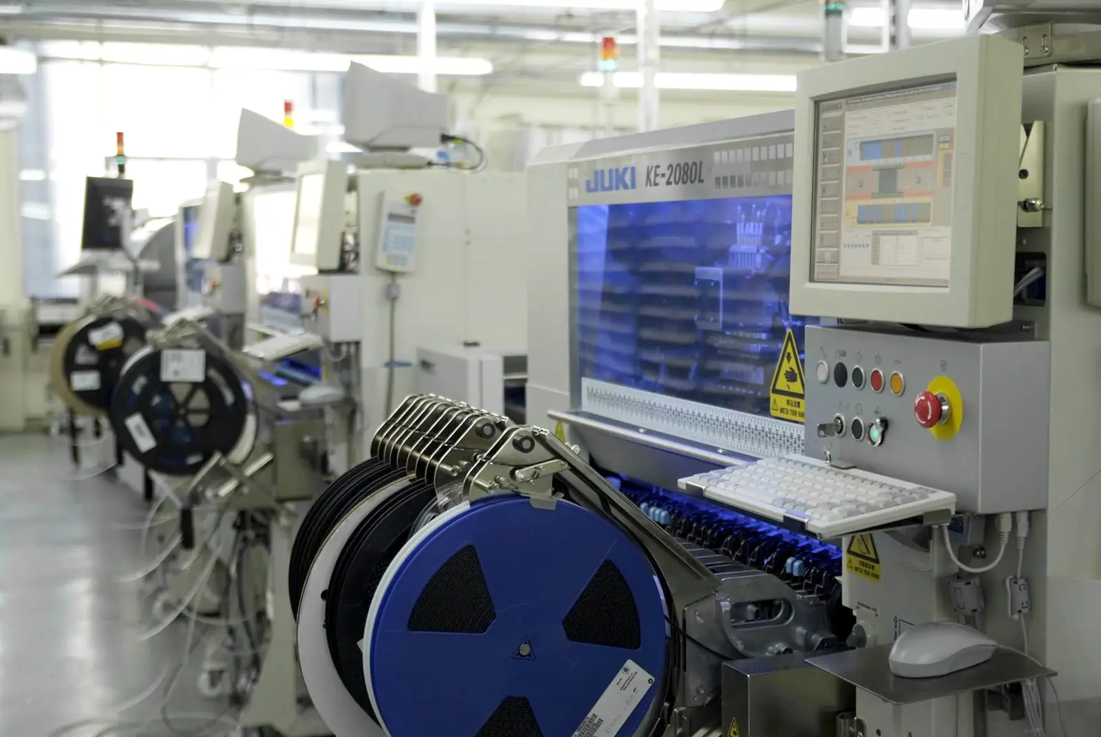
Surface mount placement machines on an electronics assembly line
All machine vision applications
Machine Vision · Electronics

PCB and Electronics Assembly Inspection

Electronics inspection uses automated optical inspection (AOI) and solder paste inspection (SPI) to check printed circuit boards at each stage of assembly: paste deposits, component placement, polarity and solder joints. Faults are found while a board can still be reworked cheaply.

PCB & Electronics Inspection at a glance

What it finds
Missing, wrong, shifted, tombstoned and reversed components, solder bridges, insufficient and excess solder.
Where it sits
After paste printing (SPI), before and after reflow (AOI), after wave or selective solder, and at final assembly.
Standard
Acceptability judged against IPC-A-610 classes and your own workmanship criteria.
What you get
Defects located on the board image for rework, and process data to fix the cause.
Definition

What is automated optical inspection?

Automated optical inspection (AOI) images an assembled circuit board and compares every component and joint with what the design and workmanship standard require. Solder paste inspection (SPI) does the same for the paste deposits before components are placed, usually in 3D.

Inspection at several points in the line matters because most solder defects start with the paste. Catching a bad print before placement costs almost nothing; finding the same fault in a finished product costs a great deal.

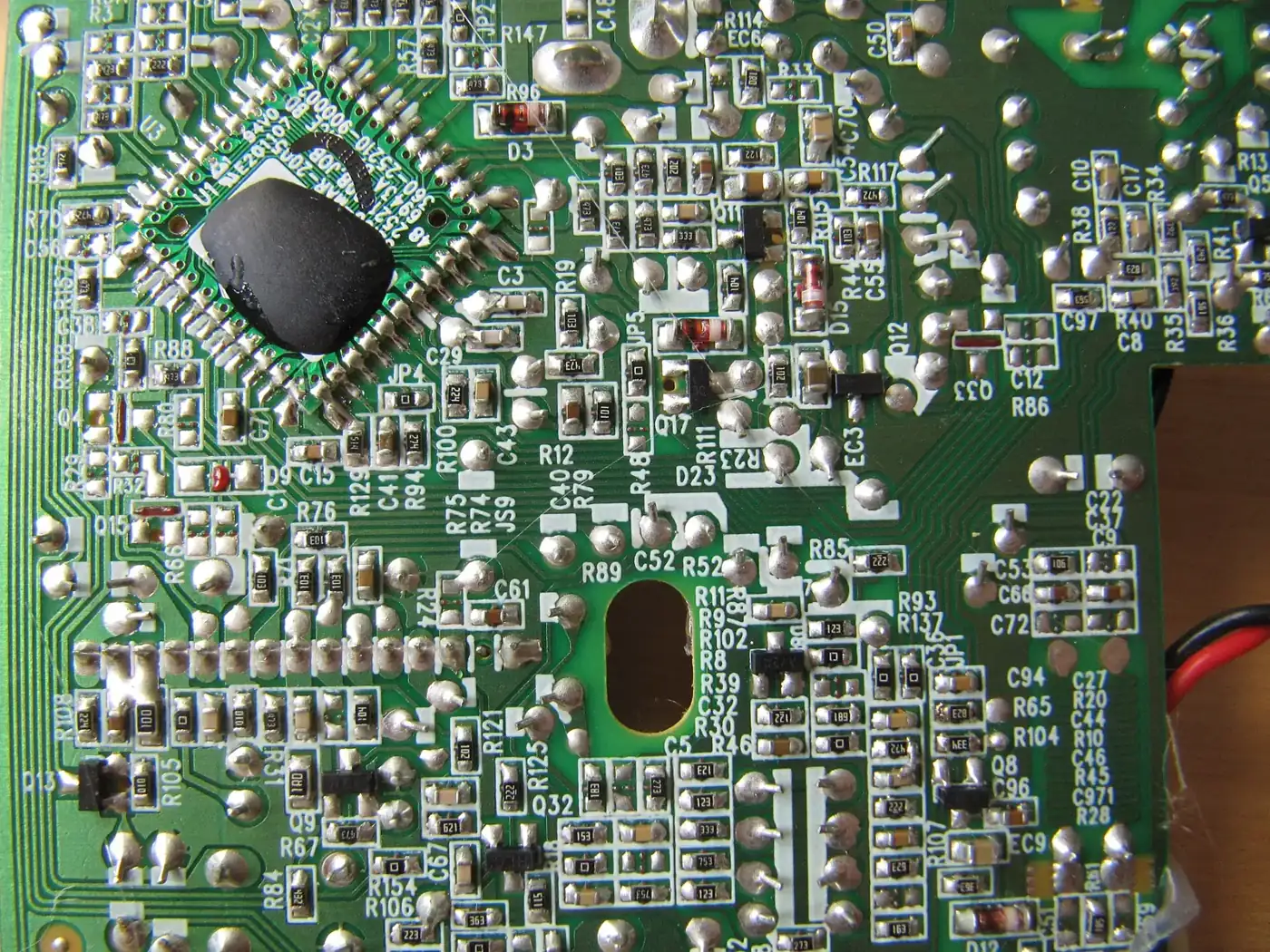
Close-up of a densely populated printed circuit board
Dense boards leave no room for a manual check. Every part and joint needs the same inspection, every time.
The problem

Why electronics needs automated inspection

  • Modern boards carry hundreds of tiny components that people cannot check reliably.
  • Solder defects are often too small to see without magnification.
  • Reversed polarity and wrong-value parts pass a quick visual check.
  • Faults found at test or in the field cost far more to fix than at the line.
  • Customers and standards require documented inspection.
How it works

How pcb & electronics inspection works, step by step

STEP 1PasteSTEP 2PlaceSTEP 3SolderSTEP 4ReviewSTEP 5Improve
  1. STEP 1

    Inspect the paste

    Solder paste inspection measures the volume, area, height and position of every deposit after printing.

  2. STEP 2

    Check placement

    Pre-reflow AOI confirms parts are present, correct and aligned before soldering fixes any mistake in place.

  3. STEP 3

    Inspect the joints

    Post-reflow AOI checks solder joints, bridges, polarity and tombstoning with multi-angle lighting.

  4. STEP 4

    Review and rework

    An operator reviews flagged locations on screen and sends real defects to rework.

  5. STEP 5

    Fix the process

    Defect data is linked back to the printer, placement machine or oven so the cause is corrected.

The technology

Methods that make it reliable

3D solder paste inspection

Measures paste height and volume, not just area, which is the strongest early predictor of solder joint quality.

Multi-angle lighting

Coloured light from several angles reveals the shape of solder fillets, so joint quality can be judged from the image.

Polarity and OCR

Reads component markings and checks polarity marks so reversed or wrong-value parts are caught.

UV coating inspection

Conformal coatings with a UV tracer glow under UV light, so coverage and keep-out areas can be checked.

Capabilities

What it can check

  • Solder paste volume and position
  • Missing components
  • Wrong components
  • Polarity and orientation
  • Placement offset and skew
  • Tombstoning and billboarding
  • Solder bridges
  • Insufficient and excess solder
  • Conformal coating coverage
Industries

Where it is used

Electronics manufacturing servicesAutomotive electronicsIndustrial controlsConsumer electronicsPower electronicsMedical electronics
Sample projects

How a project is scoped

Two example project scopes showing how the station, the checks and the outputs are defined. Every plant is different, so the final configuration is confirmed after a feasibility study on your own parts.

Example scope · SMT line

Post-reflow AOI with rework station

The situation: An electronics assembler inspects boards under a magnifier after reflow and misses intermittent faults.

Station
Inline AOI after the reflow oven, review station beside it
Checks
Presence, polarity, offset, bridges and insufficient solder
Output
Defects shown on the board image for rework
Extra
Defect trends per feeder and nozzle to the placement team
Example scope · Final assembly

Connector and label check before boxing

The situation: A controls manufacturer ships assembled units and receives returns for missing connectors.

Station
Camera at the final assembly bench
Checks
Connectors fitted, jumpers set, serial label present and readable
Output
Unit cannot be boxed until it passes
Extra
Image saved against each serial number
What is in the system

Typical components

  • AOI and SPI inspection systems
  • High-resolution area-scan cameras
  • Multi-angle coloured lighting
  • UV lighting for coatings
  • Conveyor and board handling
  • Review and rework software

Cameras and lenses, supplied locally

Industrial cameras, lenses, line-scan cameras and code readers are available through our machine vision catalog, quoted with delivery to Sri Lanka. We select the hardware for your application during the feasibility study.

Browse the hardware catalog
How we work

Proven on your parts before you commit

Every product, surface and line behaves differently under a camera, so every project starts with evidence from your own material.

  1. PHASE 1

    Discovery

    A site visit to understand your product, line speed, quality criteria and where the check should sit.

  2. PHASE 2

    Feasibility study

    We image your good and defective samples and show what the system can reliably detect. This is the go or no-go.

  3. PHASE 3

    Pilot station

    One station on one line, running beside your inspectors until results match and your team trusts them.

  4. PHASE 4

    Rollout and support

    More lines, integration with your PLC and systems, and local support from our Sri Lankan engineering team.

FAQ

PCB & Electronics Inspection: common questions

What is the difference between SPI and AOI?

+

SPI inspects solder paste after printing and before components are placed, usually measuring in 3D. AOI inspects components and solder joints, before reflow for placement and after reflow for soldering.

What is IPC-A-610?

+

IPC-A-610 is the widely used industry standard for the acceptability of electronic assemblies. It defines what acceptable and defective solder joints and component placements look like, in three product classes with increasing requirements.

Where in the line should inspection go?

+

Post-reflow AOI is the most common starting point. Adding SPI after the printer catches the cause of most solder defects earlier. The right combination depends on board complexity and volume.

Can AOI inspect through-hole boards?

+

Yes. Through-hole components and wave or selective solder joints can be inspected, usually from the solder side, with lighting chosen for through-hole fillets.

Does AOI replace electrical testing?

+

No. AOI finds visible defects quickly and cheaply; in-circuit and functional tests check electrical behaviour. Used together, they give much better coverage than either alone.

Send us a few sample parts

Tell us what you need to check and share some good and faulty samples. We will show you what a camera can reliably see before you commit to anything.

Photographs show representative plants and equipment, not Cerox installations or client sites. Diagrams by Cerox Engineering. Photo credits, via Wikimedia Commons: SMT placement line by Megger Ltd., CC BY 3.0; Populated circuit board by Loozrboy, CC BY-SA 2.0; Inspection camera in a placement machine by Nelatan, CC BY-SA 3.0.